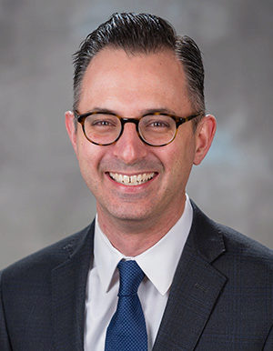
Michael Filler, an associate professor in Georgia Tech’s School of Chemical and Biomolecular Engineering (ChBE), aims to revolutionize the manufacturing of electronics, allowing them to be used in new energy, health, infrastructure, aerospace, and military applications.
Filler can envision a future with high-performance, ultra-low cost electronics that pervade environments. For example, there could be vast sensor networks that detect radiation across entire borders or that can monitor weather patterns, fires, and tree decay in forests. Sensors on seeds in fields could dramatically improve the efficiency of farming. The walls of buildings could be filled with collections of computers powered by ambient energy.
“These hyper-scalable electronic systems will require large quantities – tons rather than grams – of nanoelectronic devices, such as transistors,” explains Filler, whose research interests include innovative approaches to understanding and engineering semiconductor nanowire growth and nanowire manufacturing. “Attempts to scale production usually sacrifice structural fidelity and destroy function.”
Filler recognizes that solving these challenges could be a long, steep climb. But given the continued deceleration of Moore’s Law – the concept that the number of transistors on a microchip doubles every 18 months or so – he believes that new approaches are a must.
“Transistors are approaching atomic sizes. They can’t get much smaller,” he says. “But, for the applications we’re envisioning, they don’t need to. We need methods to make orders-of-magnitude more transistors of the same size.”
Overcoming Imperfections
Conventional semiconductor manufacturing requires near perfection. Because transistors are embedded in silicon wafers, they can’t be easily removed. “If you make a mistake, you’re done,” he says.
Most other industries assume imperfection is a natural part of the process and have developed ways to separate defective components.
Filler believes that the solutions to the challenge of hyper-scalable electronics lies in the foundational principles of chemical engineering.
“As a chemical engineer, I’m interested in the process. Have we learned enough in the last 30 years of nanotechnology to start building electronics differently? Can we develop chemical approaches not only to build complete nanoelectronic devices, but can we also separate and purify them? In short, can we process transistors like we process molecules? I think the answers are yes.”
Nanomanufacturers have depended too much on techniques inspired by the semiconductor industry, he says. These are capable of producing small numbers of high quality devices and circuits, but not at the scale necessary for many potential uses.
In a 2017 perspective article in the Annual Review of Chemical & Biomolecular Engineering, Filler and ChBE Professors Sven Behrens and Victor Breedveld recommended new synthesis techniques, new structure- and property-based separations, carefully selected process break points, and advances in stabilization and packaging. These ideas are directly relevant to their current work toward hyper-scalable electronics.
Collaborative Approach
In addition to collaborators within ChBE, Filler’s team also includes researchers at Georgia Tech in Materials Science and Engineering, and Electric and Computer Engineering, as well as from Rutgers University and the University of Michigan.
One Michigan professor’s participation stemmed from her appearance on Filler’s Nanovation Podcast, started in 2016. “I had no idea she would have skillset so synergistic with what we’re trying to do. After the show, I invited her to be part of team.”
Filler is excited about the headway they’re making. “We’re the first to take this approach, and we’ve demonstrated enough key components that people can more concretely see what we’re talking about. We’re getting them to believe,” Filler says.
Challenging Road
Filler says if he’d pursued this research focus just after joining the faculty of ChBE in 2009, “I would have never gotten tenure. It would have taken too long to change hearts and minds.”
But he’s excited now to have the academic freedom to pursue ideas that could change the world. “That’s why the tenure safety net exists. I don’t have answers to all of this yet. It’s going to take a few years. But this is where we’re going and we believe that by fundamentally rethinking the process there are exciting new things we can do,” he says.
After earning his BS in chemical engineering from Cornell University in 2000, Filler enrolled in Stanford University where he earned his PhD in 2006. After a year as a staff scientist in industry, he completed his postdoctoral studies at California Institute of Technology, where he focused on nanoscience and solar energy.
Filler has been recognized for his research and teaching with the National Science Foundation CAREER Award, Georgia Tech Sigma Xi Young Faculty Award, CETL/BP Junior Faculty Teaching Excellence Award, and AVS Dorothy M. and Earl S. Hoffman Award. He is also Georgia Tech’s Traylor Faculty Fellow.
A native of Washington D.C., Filler has no other family in the sciences or engineering. While his brother is an artist, his mother was a teacher, and his father a lawyer. “I decided I didn’t want to be a lawyer because they have to write all the time. Now that’s all I do,” he jokes.
Brad Dixon, braddixon@gatech.edu